
技术专栏
RK3568开发板安卓系统之驱动调试(四)

4 驱动调试
4.1 电源配置
RK GPIO编号说明
A组: A0-A7对应0-7B组: B0-B7对应8-15C组: C0-C7对应16-23D组: D0-D7对应24-31
GPIO编号计算方法:
例如:GPIO4_C4 = 4*32+16+4 = 148
4.1.1 查看原理图
4.1.2 获取需要的配置信息,并在dts里配置
通过查看原理图,获取到相应的信息,然后在dts里配置
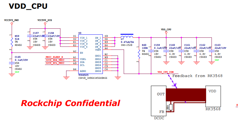
1、RK809和TCS4525是挂在I2C0下。输出电压VDD_CPU为0.9V, dts配置如下
    vdd_cpu: tcs4525@1c {
        compatible = "tcs,tcs452x";
        reg = <0x1c>;
        vin-supply = <&vcc5v0_sys>;
        regulator-compatible = "fan53555-reg";
        regulator-name = "vdd_cpu";
        ...
        regulator-init-microvolt = <900000>;
        ...
    };
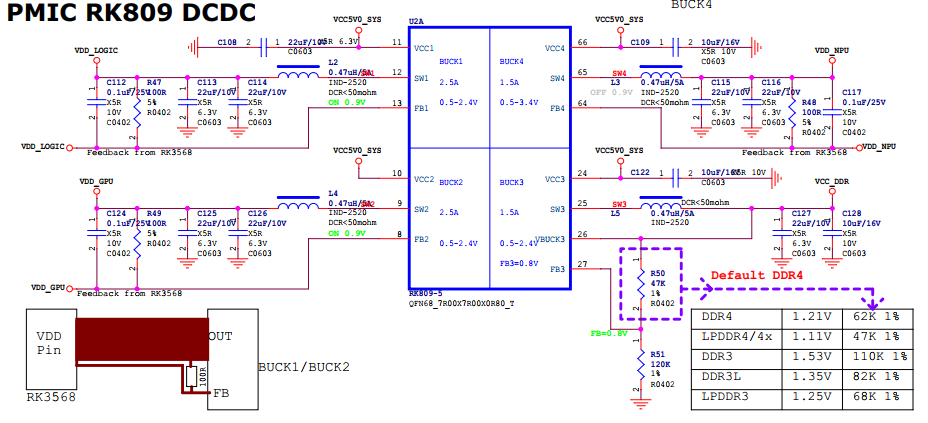
2、RK809各输入电压的输入源
| 输入电压 | 输入源 |
|---|---|
| VCC1 | VCC5V0_SYS |
| VCC2 | VCC5V0_SYS |
| VCC3 | VCC5V0_SYS |
| VCC4 | VCC5V0_SYS |
| VCC5 | VCC3V3_SYS |
| VCC6 | VCC3V3_SYS |
| VCC7 | VCC3V3_SYS |
| VCC8 | VCC3V3_SYS |
| VCC9 | VCC3V3_SYS |
dts配置如下:
    vcc1-supply = <&vcc5v0_SYS>;
    vcc2-supply = <&vcc5v0_SYS>;
    vcc3-supply = <&vcc5v0_SYS>;
    vcc4-supply = <&vcc5v0_SYS>;
    vcc5-supply = <&vcc3v3_sys>;
    vcc6-supply = <&vcc3v3_sys>;
    vcc7-supply = <&vcc3v3_sys>;
    vcc8-supply = <&vcc3v3_sys>;
    vcc9-supply = <&vcc3v3_sys>;
通过查看原理图,VCC5V0_SYS是底板给的,VCC3V3_SYS是由VCC5V0_SYS转的
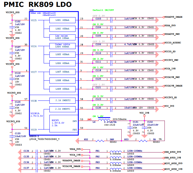
3、RK809输出电压名及其电压值
| 电源名称 | 电压值 | |
|---|---|---|
| BUCK1 | VDD_LOGIC | 0.9V |
| BUCK2 | VDD_GPU | 0.9V |
| BUCK3 | VCC_DDR | 硬件调节 |
| BUCK4 | VDD_NPU | 0.9V |
| LDO1 | VDDA0V9_IMAGE | 0.9V |
| LDO2 | VDDA_0V9 | 0.9V |
| LDO3 | VDDA0V9_PMU | 0.9V |
| LDO4 | VCCIO_ACODEC | 3.3V |
| LDO5 | VCCIO_SD | 1.8-3.3V |
| LDO6 | VCC3V3_PMU | 3.3V |
| LDO7 | VCCA_1V8 | 1.8V |
| LDO8 | VCCA1V8_PMU | 1.8V |
| LDO9 | VCCA1V8_IMAGE | 1.8V |
| SWCUT1 | VCC_3V3 | 3.3V |
| SWCUT2 | VCC3V3_SD | 3.3V |
| BUCK5 | VCC_1V8 | 1.8V |
dts里配置
regulators {
vdd_logic: DCDC_REG1 {
regulator-always-on;
regulator-boot-on;
regulator-min-microvolt = <500000>;
regulator-max-microvolt = <1350000>;
regulator-init-microvolt = <900000>;
regulator-ramp-delay = <6001>;
regulator-initial-mode = <0x2>;
regulator-name = "vdd_logic";
regulator-state-mem {
regulator-off-in-suspend;
};
};
vdd_gpu: DCDC_REG2 {
regulator-always-on;
regulator-boot-on;
regulator-min-microvolt = <500000>;
regulator-max-microvolt = <1350000>;
regulator-init-microvolt = <900000>;
regulator-ramp-delay = <6001>;
regulator-initial-mode = <0x2>;
regulator-name = "vdd_gpu";
regulator-state-mem {
regulator-off-in-suspend;
};
};
vcc_ddr: DCDC_REG3 {
regulator-always-on;
regulator-boot-on;
regulator-initial-mode = <0x2>;
regulator-name = "vcc_ddr";
regulator-state-mem {
regulator-on-in-suspend;
};
};
vdd_npu: DCDC_REG4 {
regulator-always-on;
regulator-boot-on;
regulator-min-microvolt = <500000>;
regulator-max-microvolt = <1350000>;
regulator-init-microvolt = <900000>;
regulator-ramp-delay = <6001>;
regulator-initial-mode = <0x2>;
regulator-name = "vdd_npu";
regulator-state-mem {
regulator-off-in-suspend;
};
};
vdda0v9_image: LDO_REG1 {
regulator-boot-on;
regulator-always-on;
regulator-min-microvolt = <900000>;
regulator-max-microvolt = <900000>;
regulator-name = "vdda0v9_image";
regulator-state-mem {
regulator-off-in-suspend;
};
};
vdda_0v9: LDO_REG2 {
regulator-always-on;
regulator-boot-on;
regulator-min-microvolt = <900000>;
regulator-max-microvolt = <900000>;
regulator-name = "vdda_0v9";
regulator-state-mem {
regulator-off-in-suspend;
};
};
vdda0v9_pmu: LDO_REG3 {
regulator-always-on;
regulator-boot-on;
regulator-min-microvolt = <900000>;
regulator-max-microvolt = <900000>;
regulator-name = "vdda0v9_pmu";
regulator-state-mem {
regulator-on-in-suspend;
regulator-suspend-microvolt = <900000>;
};
};
vccio_acodec: LDO_REG4 {
regulator-always-on;
regulator-boot-on;
regulator-min-microvolt = <3300000>;
regulator-max-microvolt = <3300000>;
regulator-name = "vccio_acodec";
regulator-state-mem {
regulator-off-in-suspend;
};
};
vccio_sd: LDO_REG5 {
regulator-always-on;
regulator-boot-on;
regulator-min-microvolt = <1800000>;
regulator-max-microvolt = <3300000>;
regulator-name = "vccio_sd";
regulator-state-mem {
regulator-off-in-suspend;
};
};
vcc3v3_pmu: LDO_REG6 {
regulator-always-on;
regulator-boot-on;
regulator-min-microvolt = <3300000>;
regulator-max-microvolt = <3300000>;
regulator-name = "vcc3v3_pmu";
regulator-state-mem {
regulator-on-in-suspend;
regulator-suspend-microvolt = <3300000>;
};
};
vcca_1v8: LDO_REG7 {
regulator-always-on;
regulator-boot-on;
regulator-min-microvolt = <1800000>;
regulator-max-microvolt = <1800000>;
regulator-name = "vcca_1v8";
regulator-state-mem {
regulator-off-in-suspend;
};
};
vcca1v8_pmu: LDO_REG8 {
regulator-always-on;
regulator-boot-on;
regulator-min-microvolt = <1800000>;
regulator-max-microvolt = <1800000>;
regulator-name = "vcca1v8_pmu";
regulator-state-mem {
regulator-on-in-suspend;
regulator-suspend-microvolt = <1800000>;
};
};
vcca1v8_image: LDO_REG9 {
regulator-always-on;
regulator-boot-on;
regulator-min-microvolt = <1800000>;
regulator-max-microvolt = <1800000>;
regulator-name = "vcca1v8_image";
regulator-state-mem {
regulator-off-in-suspend;
};
};
vcc_1v8: DCDC_REG5 {
regulator-always-on;
regulator-boot-on;
regulator-min-microvolt = <1800000>;
regulator-max-microvolt = <1800000>;
regulator-name = "vcc_1v8";
regulator-state-mem {
regulator-off-in-suspend;
};
};
vcc_3v3: SWITCH_REG1 {
regulator-always-on;
regulator-boot-on;
regulator-name = "vcc_3v3";
regulator-state-mem {
regulator-off-in-suspend;
};
};
vcc3v3_sd: SWITCH_REG2 {
regulator-always-on;
regulator-boot-on;
regulator-name = "vcc3v3_sd";
regulator-state-mem {
regulator-off-in-suspend;
};
};
};
在原有配置的基础上增加、删除、修改4 驱动调试
在原有配置的基础上增加、删除、修改4.1 电源配置
RK GPIO编号说明
A组: A0-A7对应0-7
B组: B0-B7对应8-15
C组: C0-C7对应16-23
D组: D0-D7对应24-31
GPIO编号计算方法:
例如:GPIO4_C4 = 4*32+16+4 = 148
4.1.1 查看原理图
4.1.2 获取需要的配置信息,并在dts里配置
通过查看原理图,获取到相应的信息,然后在dts里配置
1、RK809和TCS4525是挂在I2C0下。输出电压VDD_CPU为0.9V, dts配置如下
vdd_cpu: tcs4525@1c {
compatible = "tcs,tcs452x";
reg = <0x1c>;
vin-supply = <&vcc5v0_sys>;
regulator-compatible = "fan53555-reg";
regulator-name = "vdd_cpu";
...
regulator-init-microvolt = <900000>;
...
};
2、RK809各输入电压的输入源
| 输入电压 | 输入源 |
| ————- | —————- |
| VCC1 | VCC5V0_SYS |
| VCC2 | VCC5V0_SYS |
| VCC3 | VCC5V0_SYS |
| VCC4 | VCC5V0_SYS |
| VCC5 | VCC3V3_SYS |
| VCC6 | VCC3V3_SYS |
| VCC7 | VCC3V3_SYS |
| VCC8 | VCC3V3_SYS |
| VCC9 | VCC3V3_SYS |
dts配置如下:
vcc1-supply = <&vcc5v0_SYS>;
vcc2-supply = <&vcc5v0_SYS>;
vcc3-supply = <&vcc5v0_SYS>;
vcc4-supply = <&vcc5v0_SYS>;
vcc5-supply = <&vcc3v3_sys>;
vcc6-supply = <&vcc3v3_sys>;
vcc7-supply = <&vcc3v3_sys>;
vcc8-supply = <&vcc3v3_sys>;
vcc9-supply = <&vcc3v3_sys>;
通过查看原理图,VCC5V0_SYS是底板给的,VCC3V3_SYS是由VCC5V0_SYS转的
3、RK809输出电压名及其电压值
| | 电压名称 | 电压值 |
| ———-| —————— | —————|
| BUCK1 | VDD_LOGIC | 0.9V |
| BUCK2 | VDD_GPU | 0.9V |
| BUCK3 | VCC_DDR | 硬件调节 |
| BUCK4 | VDD_NPU | 0.9V |
| LDO1 | VDDA0V9_IMAGE| 0.9V |
| LDO2 | VDDA_0V9 | 0.9V |
| LDO3 | VDDA0V9_PMU | 0.9V |
| LDO4 | VCCIO_ACODEC | 3.3V |
| LDO5 | VCCIO_SD | 1.8-3.3V |
| LDO6 | VCC3V3_PMU | 3.3V |
| LDO7 | VCCA_1V8 | 1.8V |
| LDO8 | VCCA1V8_PMU | 1.8V |
| LDO9 | VCCA1V8_IMAGE| 1.8V |
| SWCUT1 | VCC_3V3 | 3.3V |
| SWCUT2 | VCC3V3_SD | 3.3V |
| BUCK5 | VCC_1V8 | 1.8V |
dts里配置
regulators {
vdd_logic: DCDC_REG1 {
regulator-always-on;
regulator-boot-on;
regulator-min-microvolt = <500000>;
regulator-max-microvolt = <1350000>;
regulator-init-microvolt = <900000>;
regulator-ramp-delay = <6001>;
regulator-initial-mode = <0x2>;
regulator-name = "vdd_logic";
regulator-state-mem {
regulator-off-in-suspend;
};
};
vdd_gpu: DCDC_REG2 {
regulator-always-on;
regulator-boot-on;
regulator-min-microvolt = <500000>;
regulator-max-microvolt = <1350000>;
regulator-init-microvolt = <900000>;
regulator-ramp-delay = <6001>;
regulator-initial-mode = <0x2>;
regulator-name = "vdd_gpu";
regulator-state-mem {
regulator-off-in-suspend;
};
};
vcc_ddr: DCDC_REG3 {
regulator-always-on;
regulator-boot-on;
regulator-initial-mode = <0x2>;
regulator-name = "vcc_ddr";
regulator-state-mem {
regulator-on-in-suspend;
};
};
vdd_npu: DCDC_REG4 {
regulator-always-on;
regulator-boot-on;
regulator-min-microvolt = <500000>;
regulator-max-microvolt = <1350000>;
regulator-init-microvolt = <900000>;
regulator-ramp-delay = <6001>;
regulator-initial-mode = <0x2>;
regulator-name = "vdd_npu";
regulator-state-mem {
regulator-off-in-suspend;
};
};
vdda0v9_image: LDO_REG1 {
regulator-boot-on;
regulator-always-on;
regulator-min-microvolt = <900000>;
regulator-max-microvolt = <900000>;
regulator-name = "vdda0v9_image";
regulator-state-mem {
regulator-off-in-suspend;
};
};
vdda_0v9: LDO_REG2 {
regulator-always-on;
regulator-boot-on;
regulator-min-microvolt = <900000>;
regulator-max-microvolt = <900000>;
regulator-name = "vdda_0v9";
regulator-state-mem {
regulator-off-in-suspend;
};
};
vdda0v9_pmu: LDO_REG3 {
regulator-always-on;
regulator-boot-on;
regulator-min-microvolt = <900000>;
regulator-max-microvolt = <900000>;
regulator-name = "vdda0v9_pmu";
regulator-state-mem {
regulator-on-in-suspend;
regulator-suspend-microvolt = <900000>;
};
};
vccio_acodec: LDO_REG4 {
regulator-always-on;
regulator-boot-on;
regulator-min-microvolt = <3300000>;
regulator-max-microvolt = <3300000>;
regulator-name = "vccio_acodec";
regulator-state-mem {
regulator-off-in-suspend;
};
};
vccio_sd: LDO_REG5 {
regulator-always-on;
regulator-boot-on;
regulator-min-microvolt = <1800000>;
regulator-max-microvolt = <3300000>;
regulator-name = "vccio_sd";
regulator-state-mem {
regulator-off-in-suspend;
};
};
vcc3v3_pmu: LDO_REG6 {
regulator-always-on;
regulator-boot-on;
regulator-min-microvolt = <3300000>;
regulator-max-microvolt = <3300000>;
regulator-name = "vcc3v3_pmu";
regulator-state-mem {
regulator-on-in-suspend;
regulator-suspend-microvolt = <3300000>;
};
};
vcca_1v8: LDO_REG7 {
regulator-always-on;
regulator-boot-on;
regulator-min-microvolt = <1800000>;
regulator-max-microvolt = <1800000>;
regulator-name = "vcca_1v8";
regulator-state-mem {
regulator-off-in-suspend;
};
};
vcca1v8_pmu: LDO_REG8 {
regulator-always-on;
regulator-boot-on;
regulator-min-microvolt = <1800000>;
regulator-max-microvolt = <1800000>;
regulator-name = "vcca1v8_pmu";
regulator-state-mem {
regulator-on-in-suspend;
regulator-suspend-microvolt = <1800000>;
};
};
vcca1v8_image: LDO_REG9 {
regulator-always-on;
regulator-boot-on;
regulator-min-microvolt = <1800000>;
regulator-max-microvolt = <1800000>;
regulator-name = "vcca1v8_image";
regulator-state-mem {
regulator-off-in-suspend;
};
};
vcc_1v8: DCDC_REG5 {
regulator-always-on;
regulator-boot-on;
regulator-min-microvolt = <1800000>;
regulator-max-microvolt = <1800000>;
regulator-name = "vcc_1v8";
regulator-state-mem {
regulator-off-in-suspend;
};
};
vcc_3v3: SWITCH_REG1 {
regulator-always-on;
regulator-boot-on;
regulator-name = "vcc_3v3";
regulator-state-mem {
regulator-off-in-suspend;
};
};
vcc3v3_sd: SWITCH_REG2 {
regulator-always-on;
regulator-boot-on;
regulator-name = "vcc3v3_sd";
regulator-state-mem {
regulator-off-in-suspend;
};
};
};
声明:本文内容由易百纳平台入驻作者撰写,文章观点仅代表作者本人,不代表易百纳立场。如有内容侵权或者其他问题,请联系本站进行删除。
红包
1
收藏
评论
打赏
- 分享
- 举报
 微信扫码分享
 QQ好友
QQ好友
评论
0个
手气红包
 暂无数据
暂无数据相关专栏
-
浏览量:4899次2022-10-11 10:48:08
-
浏览量:8119次2022-10-08 14:00:42
-
浏览量:3482次2022-09-30 16:48:25
-
浏览量:9330次2022-10-13 19:26:04
-
浏览量:11553次2022-10-12 09:28:15
-
浏览量:12881次2022-10-09 15:56:41
-
浏览量:12205次2022-10-10 11:27:15
-
浏览量:6683次2022-10-14 08:34:42
-
浏览量:8866次2022-10-09 10:20:09
-
浏览量:6273次2022-09-30 16:40:59
-
浏览量:10593次2022-10-17 11:49:55
-
浏览量:13886次2022-10-18 09:33:58
-
浏览量:9256次2022-10-10 20:15:42
-
浏览量:3713次2022-09-30 16:46:03
-
浏览量:7473次2022-10-08 13:56:28
-
浏览量:3821次2022-10-28 09:28:29
-
浏览量:4140次2021-06-15 09:44:15
-
浏览量:10736次2022-06-11 10:47:27
-
浏览量:36045次2022-06-11 11:06:24
关于作者

万万没想到
平安顺遂
原创26
阅读17.8w
收藏5
点赞7
评论2


切换马甲
上一页
下一页
打赏用户
共 0 位
我要创作
分享技术经验,可获取创作收益
分类专栏
-
26篇
热门专栏
- 直播 | 瑞芯微携手百度飞桨,详解基于RK3588的Paddle2RKNN部署优化
- 中国芯好消息!瑞芯微再次荣获中国芯评选“最佳市场表现奖”
- 上糖!RK3288率先支持安卓5.0 Lollipop,请你吃棒棒糖咯~
- 易百纳专栏皮肤上线,快来选择你喜欢的皮肤吧!!!
- 易百纳EulerCar 征战智能清障赛道 | 2026 无人系统挑战赛,奖金 +基金 +实习三重机遇
- rv1126移植opencv库
- RK3588部署yolov7记录
- 【活动来了!快参加!】年底了,让我任性一次!RK3288芯数码0元抢!
- 南京启诺和旷视科技达成战略合作,聚焦AI智能,携手产业共赢!
- 易百纳新品上市!海思Hi3516CV610主控平台,高性能IPC解决方案
置顶时间设置
结束时间
删除原因
-
广告/SPAM
-
恶意灌水
-
违规内容
-
文不对题
-
重复发帖
打赏作者
万万没想到
您的支持将鼓励我继续创作!
打赏金额:
¥1
¥5
¥10
¥50
¥100
支付方式:
 微信支付
微信支付
举报反馈
举报类型
- 内容涉黄/赌/毒
- 内容侵权/抄袭
- 政治相关
- 涉嫌广告
- 侮辱谩骂
- 其他
详细说明
审核成功
发布时间设置
发布时间:
请选择发布时间设置
是否关联周任务-专栏模块
审核失败
失败原因
请选择失败原因
备注
请输入备注


关注公众号
联系我们
社区问题咨询:Ebaina-CN
定制需求咨询:xxqk158820
社区问题咨询:Ebaina-CN
定制需求咨询:xxqk158820
回顶部