
详解NLDM/CCS library model
随着工艺节点下降到65nm以后,传统的NLDM model不再精确,Synopsys提出了基于电流源模型的Composite Current Source(CCS),集timing/power/noise于一体,精确度更高,与SPICE的误差可以达到±2%。
什么是Timing Model
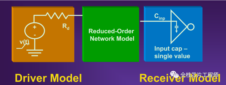
数字芯片设计,除了矿机的全定制设计外,绝大部分都是基于STD Cell的半定制设计,那么STD Cell的模型就极为重要,尤其半定制,需要把一个std cell看成block box,只考虑其input/output pin。其input pin对外部是receiver,output pin对外部是driver。因此,对receiver/driver建立精确模型十分重要。
Timing model包含driver model、net model、receiver model三个部分,Driver model和receiver models通常通过电路仿真工具K库的, 而net model要么是根据wire-load、manhattan、star topology评估的,要么是从版图根据metal、via、contact等的寄生参数来提取的。
什么是NLDM?
即(Non-Linear Delay Model)非线性延迟模型。
先看看看老外的描述:https://www.paripath.com/blog/characterization-blog/**comparing-nldm-and-ccs-delay-models**
NLDM Driver Model
NLDM driver model characterizes input-to-output delay and output transition times with sensitivity to input transition time, output load and side input states. These characteristics are obtained using a circuit simulator with appropriate stimulus to cause output transition. Input stimulus along with input/output measurement/capture points are shown in the picture below.
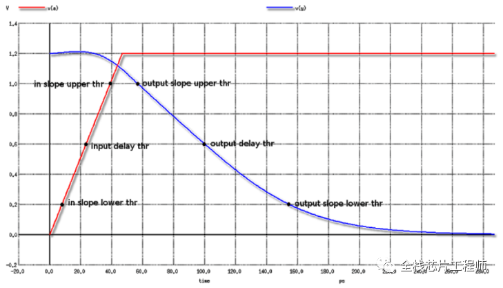
As seen in the picture, characterization software like guna measure and captures 3 points on sides of active input and active output. These three points are called delay and transition time thresholds. Difference between input delay threshold and output delay threshold is modeled as cell delay and difference between lower and upper transition times on output port is modeled as output transition time. These two parameters - delay and transition times are used to synthesize NLDM driver model shown in the picture below:
NLDM Receiver Model
NLDM receiver model is simply a single capacitor for the entire transition with no sensitivity.
Shortcomings of NLDM model
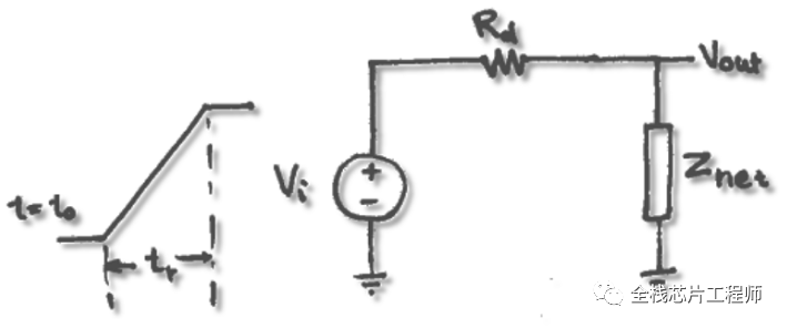
NLDM only captures 3 output points, which is not sufficient to reflect non-linearities of circuits at lower geometries (65nm and below) in synthesized driver model during static timing analysis. Classical case of this insufficiency is when driver resistance is order of magnitude less than the impedance of net it is driving (Rd
Other significant shortcoming of NLDM is in the receiver model. NLDM receiver model fails capture miller effect. This effects dominates delay calculation of STA for very small impedance nets.
也就是说,NLDM模型有如下缺点
- 仅通过3个输出点来评估延时,线性度不够精确;
- NLDM的driver model是个内阻恒定的电压源,即输出电压是时间的线性函数V(t),当65nm节点以下时,驱动线网的电阻将大得可观,模型会失真。
- NLDM的receiver model是单一的input cap,不能捕获Miller效应,对于很小的阻抗网络,Miller效应决定了延迟。
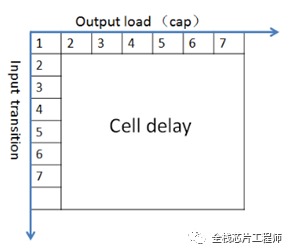
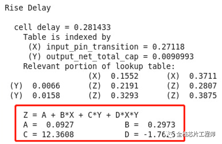
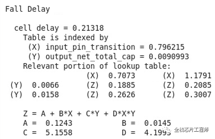
NLDM用input transition、output capacitance这两参数来查表、插值计算得到Cell delay延时及Output transition。
查找表timing部分共四个输出,前两个分别表示输出上升沿和输出下降沿的delay值,后两个分别表示输出上升沿和输出下降沿的transition time。输出的transition time则是下一级器件的input transition time。
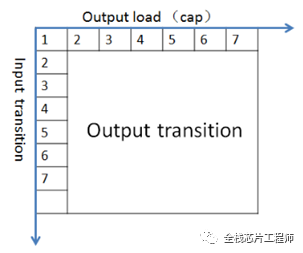
看看NLDM查表、插值计算过程:

将input transition和output capacitance这两个参数代入到std cell库中的delay lookup table,查找X 和Y左右两侧的坐标,将这四个坐标点代入二元拟合公式Z=A+ B*X + C*Y + D*X*Y,就可以得到四个二元二次方程,由这四个方程可以解出 ABCD 四个系数的值,这样就得到了一个具体的拟合公式,然后再将input transition和output capacitance代入拟合公式就可以计算出这个cell的delay值了。
什么是CCS?
即(Composite Current Source)复合电流源模型。
同样,先看看老外的描述:
CCS Driver Model
CCS driver model is characterized by capturing current waveform flowing into the load capacitor of the cell. CCS driver model also has sensitivity to input transition time, output load and side input states. CCS driver model is essentially a current source with infinite driver resistance, hence it provides better accuracy in cases where net impedance is very very high. Note, CCS timing model does not require synthesis of driver model, captured current waveform is driver model itself.
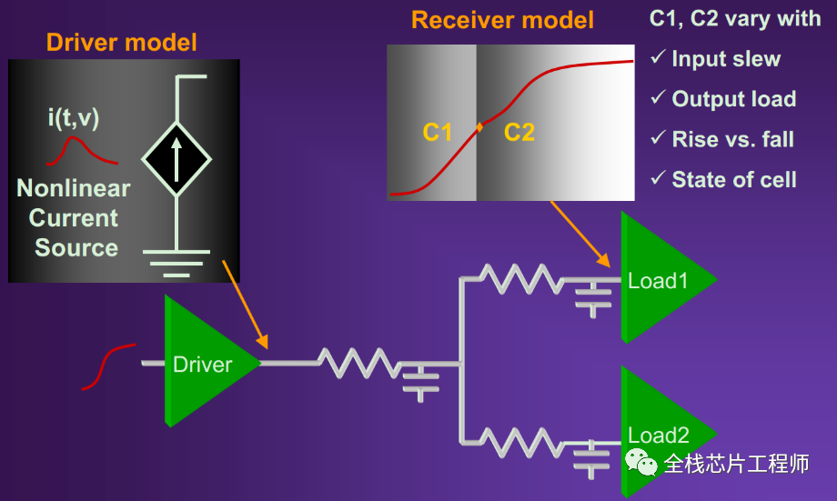
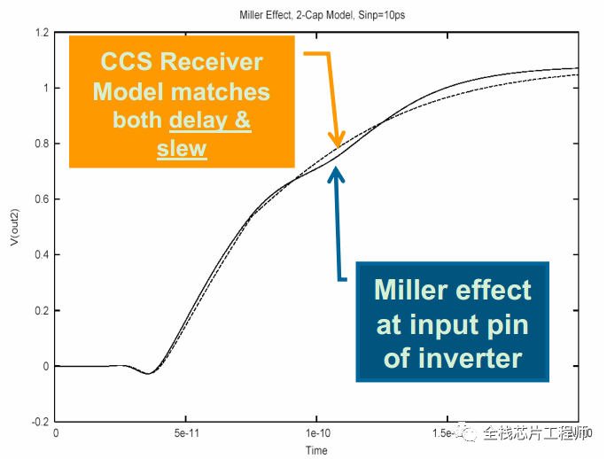
CCS Receiver Model
CCS receiver model is characterized much like NLDM receiver model with additional granularity to reflect sensitivities like miller capacitance, state of side inputs, input transition times and output load. To accurately reflect effect of miller capacitance on input capacitance and net-delay, it is divided into two parts - C1 and C2. For STA delay calculation, C1 is used in net delay calculation before receiver waveform hits delay threshold point and C2 is used in net delay calculation after receiver waveform hits delay threshold point.
也就是说,
CCS driver model是一个非线性复合电流源,电流随电压和时间而变化I(t,V),即一个具有无限驱动阻抗的电流源。
CCS receiver model为了更准确反映米勒电容,将输入电容分为C1和C2两个部分。C1用于接收波形到达延迟阈值前的net delay计算,C2用于接收波形到达延迟阈值后的net delay计算。
比如input pin的transition范围是30%到70%,那么(30%,50%)这段时间的cap值为C1,(50%,70%)这段时间的cap值为C2。
除了CCS模型,还有ECSM等模型,不再赘述。CCS、ECSM模型的数据量都大于NLDM。
典型的CCS库大约比NLDM大8-10倍。
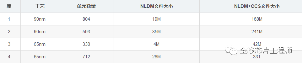
为了提供准确的电流矢量模型,CCS会存储波形,且每个波形存储10个电流值和10个时间值,共20个数字。
CCS对于每个输入转换和输出负载有20个数字,NLDM对于每个输入转换和输出负载存储2个数字。因此,与NLDM模型相比,CCS模型大小将增加10倍。
CCS lib/db里,可以同时含timing/power/noise信息。CCS lib里会看到有ccsn_first_stage/ccsn_last_stage group,分别是最前/后级管子受noise的影响。
参考文献:
《compare of CCS and NLDM》;https://www.paripath.com/blog/characterization-blog/comparing-nldm-and-ccs-delay-models,作者:paripath Inc.
===
STA概念:一文了解NLDM与CCS;
《NLDM Vs. CCS》,https://ileonsun.github.io/NLDM-VS-CCS/,作者:Leon Sun ;
部分文章索引:
芯片ECO(一)
详解GDSII文件
详解SPEF文件
详解SPI协议
详解I2C协议
详解GearBox设计原理
详解set_clock_gating_style命令
【MCU】Cortex-M3 SoC的主栈指针
低功耗设计之Multi-Bit Cell
剖析数字后端site、track、pitch的概念
Verilog中,2'b1x和2’b0x造成的仿真器、综合器的mismatch!
【剖析】傅里叶变换、拉普拉斯变换、Z变换
【剖析】傅里叶变换、拉普拉斯变换、Z变换(二)
芯片设计之CDC异步电路(五)
芯片设计之CDC异步电路(四)
芯片设计之CDC异步电路(三)
芯片设计之CDC异步电路(二)
芯片设计之CDC异步电路(一)
OCV分析计算
低功耗设计之Power Switch Cell
深度剖析“异步复位、同步撤离”
芯片后仿(二)
时钟切换clk_switch
8B/10B、64B/66B编解码(一)
8B/10B、64B/66B编解码(二)
剖析FPGA怎么实现“超前进位加法器”(一)
剖析FPGA怎么实现“超前进位加法器”(二)
FPGA原型验证-时钟门控的替换
行波进位/超前进位加法器详解
AES加密算法(一)
Cadence Voltus-功耗分析&IR-drop(一)
Cadence Voltus-功耗分析&IR-Drop(二)
Cadence Voltus-功耗分析&IR-drop(三)
Cadence Voltus-功耗分析&IR-drop(四)
感谢阅读,别走!点赞、关注、转发后再走吧
转载:全栈芯片工程师
- 分享
- 举报
 微信扫码分享
 QQ好友
QQ好友
 暂无数据
暂无数据-
浏览量:15133次2022-01-09 09:00:11
-
浏览量:2967次2022-03-08 09:00:11
-
浏览量:6251次2021-12-11 15:15:29
-
浏览量:6724次2022-03-03 09:00:09
-
浏览量:2794次2018-05-24 15:44:06
-
浏览量:2351次2024-07-31 19:46:13
-
浏览量:2565次2019-01-24 23:47:32
-
浏览量:13350次2020-12-02 22:49:48
-
浏览量:6142次2022-03-05 09:00:11
-
浏览量:3829次2020-08-20 11:09:57
-
浏览量:15230次2022-03-25 09:00:11
-
浏览量:4030次2020-08-05 20:46:02
-
浏览量:15172次2021-12-27 09:00:26
-
浏览量:6378次2024-01-12 15:00:39
-
浏览量:2331次2018-01-27 20:55:47
-
浏览量:1694次2025-04-11 11:22:04
-
浏览量:52884次2020-10-27 15:37:01
-
浏览量:17230次2020-12-02 22:47:42
-
浏览量:2804次2019-12-23 09:42:26
david
一个爱徒步的~IT民工


-
253篇
-
广告/SPAM
-
恶意灌水
-
违规内容
-
文不对题
-
重复发帖
david

 微信支付
微信支付
举报类型
- 内容涉黄/赌/毒
- 内容侵权/抄袭
- 政治相关
- 涉嫌广告
- 侮辱谩骂
- 其他
详细说明
审核成功
审核失败


关注公众号
社区问题咨询:Ebaina-CN
定制需求咨询:xxqk158820