
PVT, RC Variation & OCV
PVT:
PVT is abbreviation for Process, Voltage and Temperature. In order to make our chip to work in all possible conditions, like it should work in Siachen Glacier at -40°C and also in Sahara Desert at 60°C, we simulate it at different corners of process, voltage and temperature which IC may face after fabrication. These conditions are called as corners. All these three parameters affect the delay of the cell. We will see each and every parameter and its effect on delay in detail.
Process:
Process variation is the deviation in attributes of transistor during the fabrication.
During manufacturing a die, the area at the centre and that at the boundary will have different process variation. This happens because layers which will be getting fabricated can not be uniform all over the die. As we go away from the centre of the die, layers can differ in their sizes.
Process variation is gradual . It can not be abrupt.
Process variation is different for different technologies but is more dominant in lower node technologies (
Below are few important factors which can cause process variation;
- Wavelength of the UV light
- Manufacturing defects
The affects of process varition are listed below;
- Oxide thickness variation
- Dopant and mobility fluctuation
- Transistor width, length etc.
- RC Variation
These variations will cause the parameters like threshold voltage to change its value from expected. Threshold voltage depends on oxide thickness, source-to-body voltage and implant impurities. Consider the drain current equation for NMOS;
ID = (1/2)μnCox (W/L)(VGS – VTh)2
As we are talking about process variation, it deals with physical properties of MOSFET. So, current flowing through the channel directly depends upon mobility (μn), oxide capacitance Cox (and hence thickness of oxide i.e. tox) and ratio of width to length.
Any of these parameters change, it will result in changing the current. In other words, it will affect the delay of the circuit. Delay decreases with increase in current.
The relation between process and delay can be better understood with the following curve shown in Figure 1.
From this relation, we say that delay is more for slow process MOSFETs and it is less for fast process MOSFETs.
There are separate model files for every process corner.
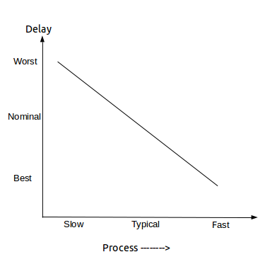
Figure 1: Process Vs Delay Graph
Voltage:
Now a days, supply voltage for a chip is very less. Lets say chip is operating at 1V. So there are chances that at certain instance of time this voltage may vary. It can go to 1.1V or 0.9V. To take care of this scenerio, we consider voltage variation.
There are multiple reasons for voltage variation. These are discussed below.
The important reason for supply voltage fluctuations is IR drop. IR drop is caused by the current flow over the parasitic resistance of the power grid. IR drop reduces the supply voltage from the required value.
The second important reason for voltage variation is supply noise caused by parasitic inductance in combination with resistance and capacitance. The current through parasitic inductance causes the voltage bounce. Both these effects together can not only lead to voltage drops but also voltage overshoot.
Supply voltage that any chip works on is given externally. It can come from DC source or some voltage regulator. Voltage regulator will not give same voltage over a period of time. It can go above or below the expected voltage and hence it will cause current to change making the circuit slower or faster than earlier.
Because of all these factors, we have to consider the voltage variation. Figure 2 shows the relation between supply voltage and delay.
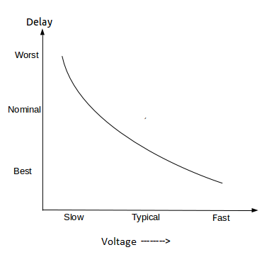
Figure 2: Voltage Vs Delay Graph
Temperature:
The temperature variation is with respect to junction and not ambient temperature. The temperature at the junction inside the chip can vary within a big range and that’s why temperature variation need to be considered. Figure 3 shows the variation of delay with respect to temperature. Delay of a cell increases with increase in temperature. But this is not true for all technology nodes. For deep sub-micron technologies this behaviour is contrary. This phenomenon is called as temperature inversion.
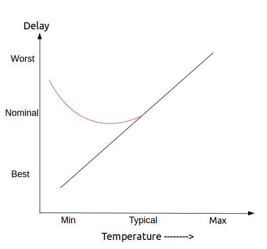
Figure 3: Temperature Vs Delay Graph
Temperature inversion: The delay depends on the output capacitance and ID current (directly proportional to Cout and inversely proportional to ID). When the temperature increases, delay also increases (due to the variation in carrier concentration and mobility). But when temperature decreases, delay variation shows different characteristics for submicron technologies. For technology nodes below 65nm, the delay will increase with decrease in temperature and it will be maximum at -40°C. This phenomena is known as “temperature inversion”.
Why Temperature inversion happens?
As temperature increases, mobility and threshold voltage start decreasing. The delay is inversely proportional to the mobility and directly proportional to the threshold voltage.
So the resultant effect from both mobility and threshold voltage decides the value of delay.
Consider the current equation of a MOSFET for better understanding;
ID = (1/2)μnCox (W/L)(VGS – VTh)2
In the higher technology node, where the supply voltage is very high, the effect of VTh is very low as (VGS – VTh) value is large. Hence mobility plays major role in deciding current. So at higher technology nodes, when the temperature increases mobility decreases and as a result the delay will increase.
At the lower technology node (specifically, less than 65nm), the supply voltage is very low, so the (VGS – VTh) difference is small and the square of this value is very small resulting reduced ID current, which increases delay at lower temperature. Where at other end above 65nm delay decreases at lower temperature.
RC Variation:
RC variation is also considered as corners for the setup and hold checks. RC variation can happen because of fabrication process and the width of metal layer can vary from the desired one.
Critical corners for Setup and Hold check
We always check our chip to work in worst scenarios. We should be very pessimistic about setup and hold checks. So consider worst case scenarios.
Setup violation can be caused if data is coming very slow. So the condition when process is slow, voltage is minimum and temperature is maximum is the worst case for setup check. Also because of temperature inversion at lower technology node, delay will increase as temperature decrease. Hence lowest temperature results in more delay. It is not compulsory that the delay at lowest temperature is always less than delay at highest temperature.
Hold violation is caused if data comes faster. So process should be faster, voltage should be maximum and temperature should be minimum.
Now if setup and hold are checked in worst corners, then the chip should work in every scenario. Still we check them in typical corners because we need to analyse power consumption. Refer following table for the worst case scenarios for setup and hold.
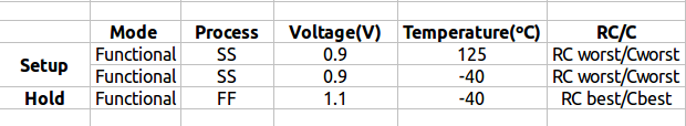
Table: Worst Scenarios for setup and hold
On Chip Variations (OCV):
Variations are of two types:
1. Global variations:
These are PVT variations that depend on external factors like Process, Supply Voltage and Temperature. ICs are fabricated in batches and hence exhibit die to die variations. Some exhibit strong process (fast switching) and weak process (slow switching). These are known as inter-chip variations.
2. Local variations:
Local variations are also variations in PVT, but these are intra-chip variations known as OCV.
Process:
All the transistors in a chip cannot be expected to have the same process. There can be variations in channel length, oxide thickness, doping concentration, metal thickness etc due to imperfections in manufacturing process like mask print, etching etc.
Voltage:
The supply voltage reaching the power pins will not be the same for all standard cells. The power network has a finite resistance. Consider two cells, one which is placed closer, and other placed far. As the interconnect length for the farther cell is more, it has more resistance and results in a higher IR drop, thereby reducing the supply voltage reaching the cell. As the voltage is less, this cell has more delay than the cell which is placed closer.
Temperature:
The transistor density within a chip is not uniform. Some regions of the chip have higher density and higher switching, resulting in a higher power dissipation. Hence the junction temperature at these regions are higher, forming localized hot spots. This variation in temperature across the chip can result in different delays.
How do you account these variations?
As a result of OCV, some cells may be fast or slow than expected. If these variations are not accounted, results may be pessimistic and can lead to setup or hold violations. In order to model these, we introduce derates. Timing derates are multiplied with the net delay and cell delay for the launch and capture clock paths. This is given as say x%. Let us consider a timing derate of 8% and how it is accounted in setup and hold analysis.
Setup analysis:
Setup check is done in worst case. The setup check is more pessimistic when the launch clock reaches late than the capture clock. Here we multiply the launch path delays with late derate of 1.08 and the capture path delays with an early derate of 0.92.
Hold analysis:
Hold check is done in best case. Hold check is more pessimistic when the launch clock reaches early than the capture clock. Here we multiply the launch path delays with an early derate of 0.92, and capture path delays with a late derate of 1.08.
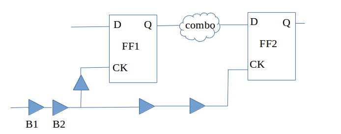
Figure 4: Timing analysis with CRPR
Consider the above path from FF1 to FF2. For setup analysis, as per the previous example, a late derate of 1.08 is applied for the launch path and an early derate of 0.92 is applied for the capture path. But what is the problem here?
The launch clock path and the capture clock path share a portion of the clock tree (B1, B2) and then diverge from the common point. This common path delays are multiplied with different derates (early and late), resulting in different delays. These cells have max delay in launch path and min delay in capture path. The same cell cannot have different delays at the same time. This results in additional pessimism which has to be removed. Here comes the need for Clock Re-convergence Pessimism Removal (CRPR) or Common Path Pessimism Removal (CPPR). This pessimism value is the difference between the max and min delay at the common clock path. To reduce pessimism, CRPR is added to required time in setup analysis and subtracted from required time in hold analysis.
原文链接:https://mp.weixin.qq.com/s/tiZwtgocE5CHZA37IO1UuA
感谢阅读,别走!点赞、关注、转发后再走吧
转载:全栈芯片工程师
- 分享
- 举报
 微信扫码分享
 QQ好友
QQ好友
 暂无数据
暂无数据-
浏览量:4637次2021-12-22 09:00:26
-
浏览量:3548次2021-12-24 09:00:17
-
浏览量:8206次2021-12-23 09:00:16
-
浏览量:7164次2021-08-10 14:13:11
-
浏览量:6089次2021-04-15 15:05:49
-
2022-10-21 14:52:47
-
浏览量:3811次2024-01-18 15:01:07
-
2024-01-05 17:19:54
-
浏览量:13708次2022-02-24 09:00:28
-
浏览量:15143次2022-01-09 09:00:11
-
2024-02-23 16:20:11
-
浏览量:5750次2022-03-02 09:00:10
-
浏览量:2969次2022-03-08 09:00:11
-
浏览量:2815次2020-08-29 21:27:46
-
浏览量:7960次2020-11-24 23:18:39
-
浏览量:9450次2020-11-24 23:02:41
-
浏览量:1872次2024-02-21 17:14:02
-
浏览量:10776次2020-08-18 21:11:17
-
浏览量:12028次2020-08-18 21:37:52
david
一个爱徒步的~IT民工


-
253篇
-
广告/SPAM
-
恶意灌水
-
违规内容
-
文不对题
-
重复发帖
david

 微信支付
微信支付
举报类型
- 内容涉黄/赌/毒
- 内容侵权/抄袭
- 政治相关
- 涉嫌广告
- 侮辱谩骂
- 其他
详细说明
审核成功
审核失败


关注公众号
社区问题咨询:Ebaina-CN
定制需求咨询:xxqk158820