
标准单元库设计(二)
Cells in generic library1. Basic gates (AND, OR, NAND, NOR, INV, EXOR, EXNOR)2. MUX3. HA, FA4. Special cells (Fillers, Tap cells, End Cap, De Caps)5. Tie Cells6. Metal Eco-able cells7. AOI8. OAI9. Boolean function cells10. Flops (Normal D flip flop, Scan-able flop with set / reset)11. Clock gatePower management cells**
Isolation cell● Used to isolate the output of OFF domain.● Allowing the floating output value of OFF domain (in off state) to be connected with the ON domain will result in- Flow of crowbar current, resulting in the increase of power consumption.
- Improper functioning of ON domain which may cause meta-stability.
● Also known as clamp cells, because they are used to clamp the intermediate voltage levels to either 0 or 1.● Isolation cells are designed either using OR gate (clamp 1) or AND gate (clamp 0).● In case of microcontroller, when the processor goes to off mode, we use isolation cells to isolate the processor core from other modules.● Isolation cells can be placed either in OFF domain or ON domain.● When there are multiple fanouts from the OFF domain placing one isolation cell in the OFF domain will isolate multiple sinks. Power must be provided from always ON supply/sink domain power supply which is challenging.● Isolation cells if placed in ON domain don’t require secondary power supply. 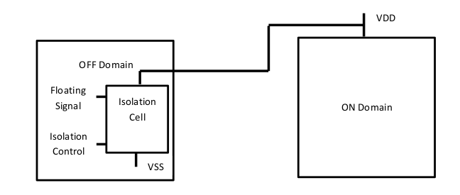 Fig2: Isolation cellLevel Shifter● Level shifter cell is used to shift a signal voltage from one voltage domain to another.● These cells are required when the chip is operating at multiple voltage domains.● The difference in voltage range may cause unreliable functioning of destination domain hence, level shifters cells are inserted in the voltage domain crossing.
  Fig3: Level shifterPower gate / switch
● The factors which are to be considered while designing power switch network are:● When they are ON, their Vt will be so low whereas when they are OFF, their Vt will be so high.● Power gates are designed with the help of multi threshold CMOS.● Power gating is a technique used in IC designs to reduce power consumption by shutting off the power to blocks of the circuit that are not in use.● Power gates are used for power gating.- Rush current: Rush current is the current drawn by a component during its initial power up to charge its internal capacitors. When a power domain is powered up from shutdown all the capacitors in the power domain starts to charge. The amount of current drawn will be huge as all the capacitors start to charge which will result in sudden rush of current. This rush current can damage the power switch network. For this we usually design the power switch network in daisy chain fashion.
- Leakage current: The number of power switches used to implement power switch network should be optimal because if more power switches are there leakage current will be more.
- Ramp up time: It is the time required to power up an off component so the power switch network should be designed in such a way that the ramp up time is less. It can be achieved by increasing the number of power switches.
Retention flop● Retention flops are always ON flops which are used to retain the data when a power domain goes to OFF mode.● Secondary power supply is used to power these flops.● A retention flop is a combination of regular flop and state saving latch.原文链接:https://mp.weixin.qq.com/s/91uIeOu6Q1MuJuJiZ5OFjg
感谢阅读,别走!点赞、关注、转发后再走吧
转载:全栈芯片工程师
- 分享
- 举报
 微信扫码分享
 QQ好友
QQ好友
 暂无数据
暂无数据-
浏览量:2971次2022-03-08 09:00:11
-
浏览量:3507次2022-03-06 09:00:09
-
浏览量:9437次2022-01-01 09:00:13
-
浏览量:3765次2020-07-20 19:36:33
-
浏览量:15147次2022-01-09 09:00:11
-
浏览量:15237次2022-03-25 09:00:11
-
浏览量:2365次2019-11-14 09:08:28
-
浏览量:7347次2022-03-26 09:00:12
-
浏览量:2999次2020-07-30 18:41:41
-
浏览量:3637次2022-01-12 09:00:12
-
浏览量:6548次2020-08-23 21:07:51
-
浏览量:4208次2022-03-01 09:00:10
-
浏览量:4195次2019-11-21 09:05:53
-
浏览量:19448次2021-01-21 11:45:55
-
浏览量:1516次2023-08-15 14:40:41
-
浏览量:2465次2019-08-08 17:11:28
-
浏览量:16263次2020-12-15 01:26:18
-
浏览量:2688次2020-07-09 10:07:51
-
浏览量:13941次2021-01-18 17:28:31
david
一个爱徒步的~IT民工


-
253篇
-
广告/SPAM
-
恶意灌水
-
违规内容
-
文不对题
-
重复发帖
david

 微信支付
微信支付
举报类型
- 内容涉黄/赌/毒
- 内容侵权/抄袭
- 政治相关
- 涉嫌广告
- 侮辱谩骂
- 其他
详细说明
审核成功
审核失败


关注公众号
社区问题咨询:Ebaina-CN
定制需求咨询:xxqk158820