
Cells in PD | PD Essentials | Physical Design
Cells in ASIC Physical Design
-
Special Cell Requirements in IC Design is to minimize the possible CMOS issues
-
More no. of transistors than are necessary for basic functioning. e.g., — To limit the Overshoots and Undershoots
-
To protect the components from destruction
-
To isolates 2 components by PN Junction
-
Common Special Cells used in CMOS IC Design:
-
Standard Cells
-
ICG Cells
-
Well taps (Tap Cells)
-
End caps
-
Filler Cells
-
Decap Cells
-
ESD Clamps
-
Spare Cells
-
Tie Cells
-
Delay Cells
-
Metrology Cells
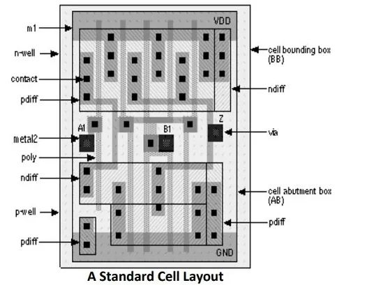
Standard Cells
-
A Standard Cell is a group of transistor and its interconnect structures that provides a Boolean logic function (e.g., AND, OR, XOR, XNOR, Inverters) or a storage function (Flip-flop or Latch)
-
Std. Cell methodology has helped designers to scale ASICs from comparatively simple single-function ICs, to complex multi-million gate SoCs
-
Cell-based methodology makes designer to focus on the implementation (physical) aspects
-
The cell's Boolean logic function is called its logical view: functional behavior is captured in the form of a truth table or Boolean algebra equation (for combinational logic), or a state transition table (for sequential logic)
-
AOIs (AND-OR-INVERTER) provide a way at the gate level to use less transistors than separate ANDs and a NORs
-
ASIC design logic builds upon a standard logic cell library, therefore, do not optimize transistors only logic gates
-
Types of Standard Cells
-
Buffers (Inverting and Non-inverting )
-
Combinational (AND, OR, NAND, NOR, AOI, OAI, OA, AO, MUX)
-
Arithmetic (XOR, full-adder, half-adder), Sequential (latches, clockgates, D-type flip/flops with any optional combination of scan input, set and reset)
-
Miscellaneous (ICG Cells, Well Taps, Tie Cells, End Caps, Decaps, Filler Cells, Spare Cells, Delay Cells, Antenna Diode, ESD diodes)
-
ICG Cells
Integrated Clock Gating Cells (ICG Cells)
- During idle modes, the clocks can be gated-off to save dynamic power dissipation on flip-flops
- Proper circuit is essential to achieve a gated clock state to prevent false glitches on clock path
- Use a combination of AND and a Latch to avoid any glitches on the clocks. A glitch can propagate a false edge on to the design
Insertion of ICG
-
Manual insertion of ICG
-
The clock gating can be implemented through logic circuits and ICG’s
-
Most of Clock Gating Cells from vendor libraries have a RTL code
-
Automated Insertion of ICG –
-
Some power aware tools insert the ICG’s through automated software algorithms
Types of Clock Gating Cells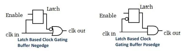
-
Latch Based Clock Gating Buffer for Neg-edge
-
The circuit employs a latch and OR gate with one input inverted
-
The output clock is always clock gated low when Enable is low
-
Latch Based Clock Gating Buffer for Pos-edge
-
The circuit employs a latch with inverted clock input and a AND gate
-
The output clock is always clock gated HIGH when Enable is low
ICG module IO’s
-
3 input ports – clock, clock enable and test
-
1 output port – clock for gated clock
-
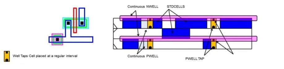
Well Taps
-
Physical only cell which helps to tie MOS Substrate and N-Wells to VDD and GND levels, and thus avoid latch-up possibilities
-
Switching circuits dump current into Well/ Substrate and if there is a high resistance between Well/ Substrate and the VDD/ GND grids the Substrate can be at different potential than VDD/ GND which causes latch-up
-
Well Tap Cells reduce resistance between VDD/ GND to wells of the Substrate
-
Tap Cells are usually placed on the Power Rails of the Standard Cells
-
Standard Cells do not have internal tap to N-well (P substrate process) to reduce design complexity of Standard Cells
-
These library cells do not have any signal connectivity
-
Hence Tap to Wells is done by external cells called "Tap cells" which are sprinkled all over Core Area at regular distance as decided by the foundry
-
More Taps reduces resistance, but will also increases core area, so we need a trade-off which will be provided by the foundry
-
Place well taps at regular intervals throughout the design with the specified distances and snaps them to legal positions
-
End Caps

-
End-cap cells are preplaced physical-only cells required to meet certaindesign rules and placed at the ends of the site rows by satisfying well tie-off requirements for the core rows
-
These library cells do not have any signal connectivity
-
They connect only to the power and ground rails once power rails are created in the design
-
They also ensure that gaps do not occur between the well and implant layers i.e. well proximity effect
-
This prevents DRC violations by satisfying well tie-off requirements for the core rows
-
Each end of the core row, left and right, can have only one end cap cell specified
-
However, you can specify a list of different end caps for inserting horizontal end cap lines, which terminate the top and bottom boundaries of objects such as macros
-
End caps have a fixed attribute and cannot be moved by optimization steps
-
A core row can be fragmented (contains gaps), since rows do not intersect objects such as power domains. For this, the tool places end cap cells on both ends of the un-fragmented segment
-
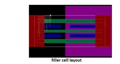
Filler Cells
-
Physical only cells which provide N-Well continuity and avoid N-Well spacing DRC
-
Filler cells are inserting for density rules, to meet Core Utilization targets and to avoid sagging of layer
-
Filler cells are inserting at the last stage of Placement and Routing
-
Some of the small cells also don’t have the Bulk/Substrate connection because of their small size (thin cells)
-
In those cases, the abutment of cells through inserting Filler Cells can connect those Substrates of small cells to VDD/ GND nets
-
i.e. those thin cells can use the bulk connection of the other cells
-
Filler cells are used to make up the Poly density (if that filler cell is having any poly structure inside), but certainly not for metal density
-
Filler cells are also useful for ECO
-
Decap Cells
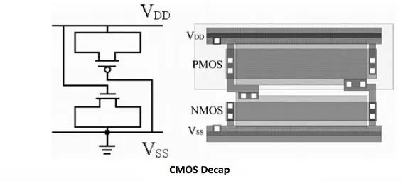
-
Decaps are on-chip decoupling capacitors (Extrinsic Capacitances) that are attached to the power mesh to decrease noise effects (dynamic I.R. Drop)
-
Supply voltage variations caused by Instantaneous Voltage Drop (IVD) lead to problems related to spurious transitions and delay variations
-
Decap cells are typically poly gate transistors where source and drain are connected to the ground rail, and the gate is connected to the power rail
-
Decap helps to smoothen out the Glitches and Ground bounce
-
3% to 8% of the core physical area is required for Decaps refered as decap density
-
It is important to place only the necessary amount of decaps since they normally come with a quite serious down-side as they are leaky devices
-
Another drawback, which many designers ignore, is the interaction of the decap cells with the package RLC network
-
Since the die is essentially a capacitor with very small R and L, and the package is a hug RL network, the more decap cells placed the more chance of tuning the circuit into its resonance frequency. That would be trouble, since both VDD and GND will be oscillating
-
NMOS Decaps are superior to PMOS decaps because of the high frequency operation and large REFF and CEFF for the same area
-
ESD Clamp
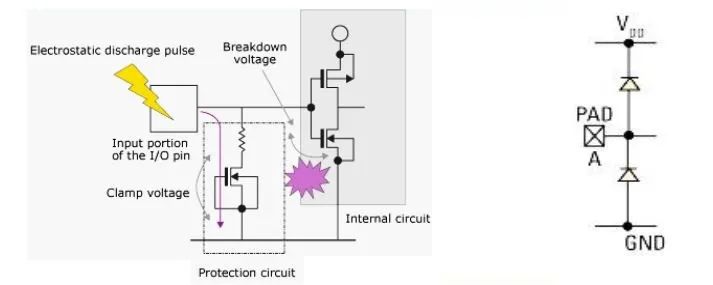
-
ESD Clamp/ ESD Diode is the primary protection device that protects against ESD surges at the I/O pad by clamping the voltage and allowing the high ESD current to be discharged safely to the ground terminal
-
The main function of ESD Clamp is to protect the Gate oxide
-
Snap back device (Diode implementation between the grounds) provides Snapback voltage (ESD Voltage) to get grounded thus the ESD current won’t be getting in to Gate
-
The design of ESD Clamp must ensure that Electrical Overstress (EOS) events do not cause failure
-
The ESD Clamp is essential for HBM, MM, and CDM
-
Spare Cells
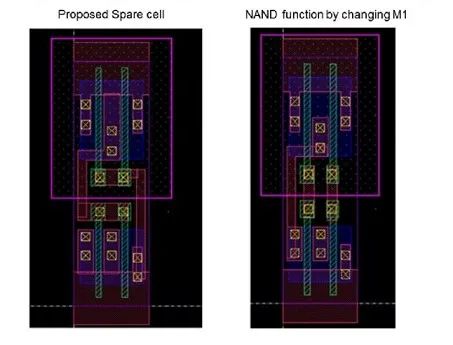
-
Pre-placed inactive (with inputs tied off) gates in the empty areas of a design (or even in the crowded areas) before tape-out (Mostly NAND Gates)
-
ECO Cells/ Spare Cells are collection of Gates coming in different sizes for doing small functional ECO and connect them with minimal mask changes called a metal-only ECO
-
Provides new functions on a design which exhibits post-production problems
-
No change is made to the diffusion layer, M1 and a contact layer only need to change
-
Disadvantages:
-
They are connected to VSS and VDD and despite having their inputs tied off, they are still drawing Static Current
-
The designer may not have the right cell in the right place at the time of the ECO
-
Tie Cells
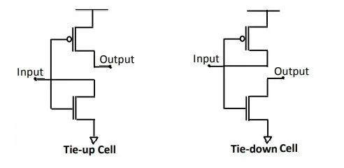
-
Tie-high and Tie-Low cells are used to connect the Gate of the transistor to either Power or Ground
-
In deep sub micron process, if the Gate is connected to Power/ Ground, the transistor might be turned ON/ OFF due to Power or Ground Bounce
-
The suggestion from foundry is to use Tie Cells for the purpose
-
The cells which require VDD, comes and connect to Tie High (so Tie High is a Power Supply Cell), while the cells which wants VSS connects itself to Tie-Low
-
Without Tie Cells, unused inputs are tied to logic-high or logic-low, and these connections are made by routing the input pin right to the Power/ Ground grid
-
With Tie Cells, unused inputs in the original netlist are tied to logic-high or logic-low, and somewhere during the physical design process, Tie Cells are inserted
-
The unused inputs are then connected to a Tie-high or Tie-low Cell
-
Delay Cells
-
Delay Cells
-
Are buffer cells with slower transition time
-
Can drive high currents
-
Are helpful in reducing Slew Rate (0-1 or 1-0 Transition Time)
-
Are of wider channel
-
Have delay starting from 20ps to few Nano seconds
-
Will have constant delay
-
Delay cell insertion is the conventional way to fix hold time violation tends to penalized in area percentage increment
-
Lesser number of delay cells are required for hold time fixing as compared to buffers but it will have area much greater than normal buffers
-
Increasing gate width reduces gate capacitance hence reduces delay, but results in higher leakage
-
It has inverter in input and a inverter in output and in between these two inverters it has a combination of a inverter and pass transistors. Pair of inverter and pass transistor provide at large delay
-
Depending on the delay of the cell, pair of inverter and pass transistor can be repeated multiple times
-
Metrology Cells
- To enable the reliable re-productivity of micro-scale devices used in high volume and low cost
- To measure and monitor the process parameters during manufacturing
- The effect of process variations during fabrication time can be identified and measured
原文链接:https://mp.weixin.qq.com/s/arI-XeOetDwYcJ83LqqBfQ
感谢阅读,别走!点赞、关注、转发后再走吧
转载:全栈芯片工程师
- 分享
- 举报
 微信扫码分享
 QQ好友
QQ好友
 暂无数据
暂无数据-
浏览量:2054次2020-11-03 14:59:08
-
浏览量:5986次2021-07-17 15:37:58
-
浏览量:9474次2021-03-16 14:44:24
-
浏览量:2032次2020-12-29 15:08:06
-
浏览量:1791次2023-04-26 16:58:30
-
浏览量:10611次2022-10-17 11:49:55
-
浏览量:1976次2020-12-14 14:30:32
-
浏览量:2794次2020-07-04 14:15:25
-
浏览量:3588次2024-01-10 10:27:15
-
浏览量:4336次2022-03-18 09:00:10
-
浏览量:2982次2022-03-08 09:00:11
-
浏览量:8209次2022-01-07 09:00:13
-
浏览量:2897次2020-09-25 14:42:36
-
浏览量:5521次2024-01-02 22:42:19
-
浏览量:12260次2020-10-13 17:41:07
-
浏览量:7355次2022-03-26 09:00:12
-
浏览量:3271次2020-11-03 11:23:20
-
浏览量:6458次2022-03-27 09:00:12
-
浏览量:5787次2022-02-01 09:00:11
david
一个爱徒步的~IT民工


-
253篇
-
广告/SPAM
-
恶意灌水
-
违规内容
-
文不对题
-
重复发帖
david

 微信支付
微信支付
举报类型
- 内容涉黄/赌/毒
- 内容侵权/抄袭
- 政治相关
- 涉嫌广告
- 侮辱谩骂
- 其他
详细说明
审核成功
审核失败


关注公众号
社区问题咨询:Ebaina-CN
定制需求咨询:xxqk158820