
【MCU】16bit CPU设计实战(二)
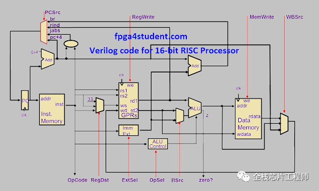
本CPU设计基于16bit RISC指令集、哈佛结构完成,架构图如下:
CPU架构
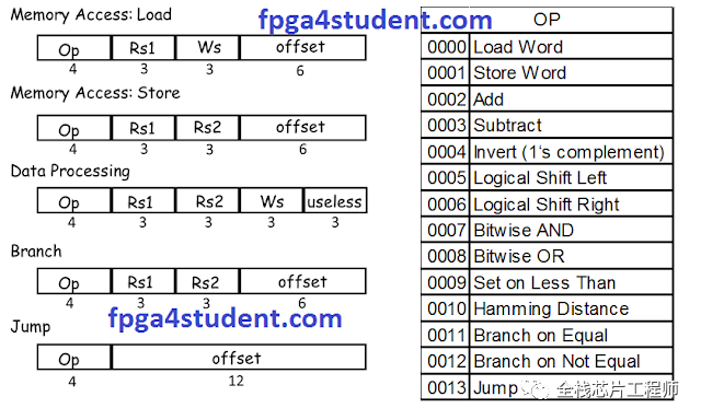
A. Memory Access Instructions
1. Load Word:
LD ws, offset(rs1) ws:=Mem16[rs1 + offset]
2. Store Word:
ST rs2, offset(rs1) Mem16[rs1 + offset]=rs2
B. Data Processing Instructions
1. Add:
ADD ws, rs1, rs2 ws:=rs1 + rs2
2. Subtract:
SUB ws, rs1, rs2 ws:=rs1 – rs2
3. Invert (1‘s complement):
INV ws, rs1 ws:=!rs1
4. Logical Shift Left:
LSL ws, rs1, rs2 ws:=rs1
5. Logical Shift Right:
LSR ws, rs1, rs2 ws:=rs1 >> rs2
6. Bitwise AND:
AND ws, rs1, rs2 ws:=rs1 • rs2
7. Bitwise OR:
OR ws, rs1, rs2 ws:=rs1 | rs2
8. Set on Less Than:
SLT ws, rs1, rs2 ws:=1 if rs1
C. Control Flow Instructions
1. Branch on Equal:
BEQ rs1, rs2, offset
Branch to (PC + 2 + (offset
2. Branch on Not Equal:
BNE rs1, rs2, offset
Branch to (PC + 2 + (offset
3. Jump: JMP offset Jump to {PC [15:13], (offset
Instruction Format of the RISC
Processor Control Unit Design:

ALU Control Unit Design:

Verilog code for the RISC processor:
1. Verilog code for Instruction Memory :
<pre style="color: rgb(0, 0, 0);font-size: 18.48px;line-height: 23.1px;"><span style="color: rgb(0, 51, 102);font-weight: bold;"></span><pre class="code-snippet__js" data-lang="cpp">```
<span class="code-snippet_outer">`include <span class="code-snippet__string">"Parameter.v"</span></span>// fpga4student.com
<span class="code-snippet_outer"><span class="code-snippet__comment">// FPGA projects, VHDL projects, Verilog projects </span></span>// Verilog code for RISC Processor
<span class="code-snippet_outer"><span class="code-snippet__comment">// Verilog code for Instruction Memory</span></span>module Instruction_Memory(
<span class="code-snippet_outer"> input[<span class="code-snippet__number">15</span>:<span class="code-snippet__number">0</span>] pc,</span>output[15:0] instruction
<span class="code-snippet_outer"><span class="code-snippet_outer">)</span>;</span><span class="code-snippet_outer"> reg [`col - <span class="code-snippet__number">1</span>:<span class="code-snippet__number">0</span>] memory [`row_i - <span class="code-snippet__number">1</span>:<span class="code-snippet__number">0</span>];</span>wire [3 : 0] rom_addr = pc[4 : 1];
<span class="code-snippet_outer"> initial</span>begin
<span class="code-snippet_outer"> $readmemb(<span class="code-snippet__string">"./test/test.prog"</span>, memory,<span class="code-snippet__number">0</span>,<span class="code-snippet__number">14</span>);</span>end
<span class="code-snippet_outer"> assign instruction = memory[rom_addr]; </span><span class="code-snippet_outer">endmodule</span>
``` #### 2. Verilog code for register file: `````` - - - - - - - - - - - - - - - - - - - - - - - - - - - - - - - - - - - - `````` 1ns / 1ps `````` fpga4student.com `````` FPGA projects, VHDL projects, Verilog projects `````` Verilog code for RISC Processor `````` Verilog code for register file `````` module GPRs( `````` input clk, `````` write port `````` input reg_write_en, `````` input [2:0] reg_write_dest, `````` input [15:0] reg_write_data, `````` port 1 `````` input [2:0] reg_read_addr_1, `````` output [15:0] reg_read_data_1, `````` port 2 `````` input [2:0] reg_read_addr_2, `````` output [15:0] reg_read_data_2 `````` ); `````` reg [15:0] reg_array [7:0]; `````` integer i; `````` write port `````` [2:0] i; `````` initial begin `````` =0;i `````` `````` end `````` always @ (posedge clk ) begin `````` begin `````` `````` end `````` end `````` `````` assign reg_read_data_1 = reg_array[reg_read_addr_1]; `````` = reg_array[reg_read_addr_2]; ``````
`````` endmodule ``` ``` ```
``` #### 3. Verilog code for Data Memory: `````` - - - - - - - - - - - - - - - - - - - - - - - - - - - - - - - - - - - - - - - - - - - - - - `````` `include "Parameter.v" `````` // fpga4student.com `````` // FPGA projects, VHDL projects, Verilog projects `````` // Verilog code for RISC Processor `````` // Verilog code for data Memory `````` module Data_Memory( `````` input clk, `````` // address input, shared by read and write port `````` input [15:0] mem_access_addr, `````` `````` // write port `````` input [15:0] mem_write_data, `````` input mem_write_en, `````` input mem_read, `````` // read port `````` output [15:0] mem_read_data `````` ); ``````
`````` reg [`col - 1:0] memory [`row_d - 1:0]; `````` integer f; `````` wire [2:0] ram_addr=mem_access_addr[2:0]; `````` initial `````` begin `````` $readmemb("./test/test.data", memory); `````` `````` f = $fopen(`filename); `````` $fmonitor(f, "time = %d\n", $time, `````` "\tmemory[0] = %b\n", memory[0], `````` "\tmemory[1] = %b\n", memory[1], `````` "\tmemory[2] = %b\n", memory[2], `````` "\tmemory[3] = %b\n", memory[3], `````` "\tmemory[4] = %b\n", memory[4], `````` "\tmemory[5] = %b\n", memory[5], `````` "\tmemory[6] = %b\n", memory[6], `````` "\tmemory[7] = %b\n", memory[7]); `````` `simulation_time; `````` $fclose(f); `````` end `````` `````` always @(posedge clk) begin `````` if (mem_write_en) `````` memory[ram_addr] `````` end `````` assign mem_read_data = (mem_read==1'b1) ? memory[ram_addr]: 16'd0; ``````
`````` endmodule ``` ``` `````` #### 4. Verilog code for ALU unit: ```
``` - - - - - - - - - - - - - - - - - - - - - - - - - - - - - - - - `````` // fpga4student.com `````` // FPGA projects, VHDL projects, Verilog projects `````` // Verilog code for RISC Processor `````` // Verilog code for ALU `````` module ALU( `````` input [15:0] a, //src1 `````` input [15:0] b, //src2 `````` input [2:0] alu_control, //function sel `````` `````` output reg [15:0] result, //result `````` output zero `````` ); ``````
`````` always @(*) `````` begin `````` case(alu_control) `````` 3'b000: result = a + b; // add `````` 3'b001: result = a - b; // sub `````` 3'b010: result = ~a; `````` 3'b011: result = a `````` 3'b100: result = a>>b; `````` 3'b101: result = a & b; // and `````` 3'b110: result = a | b; // or `````` 3'b111: begin if (a16'd1; `````` else result = 16'd0; `````` end `````` default:result = a + b; // add `````` endcase `````` end `````` assign zero = (result==16'd0) ? 1'b1: 1'b0; `````` `````` endmodule ``` ``` #### #### 5. Verilog code for ALU Control Unit of the RISC processor: `````` - - - - - - - - - - - - - - - - - - - - - - - - - `````` `timescale 1ns / 1ps `````` //fpga4student.com: FPGA projects, Verilog projects, VHDL projects `````` // Verilog code for 16-bit RISC processor `````` // ALU_Control Verilog code `````` module alu_control( ALU_Cnt, ALUOp, Opcode); `````` output reg[2:0] ALU_Cnt; `````` input [1:0] ALUOp; `````` input [3:0] Opcode; `````` wire [5:0] ALUControlIn; `````` assign ALUControlIn = {ALUOp,Opcode}; `````` always @(ALUControlIn) `````` casex (ALUControlIn) `````` 6'b10xxxx: ALU_Cnt=3'b000; `````` 6'b01xxxx: ALU_Cnt=3'b001; `````` 6'b000010: ALU_Cnt=3'b000; `````` 6'b000011: ALU_Cnt=3'b001; `````` 6'b000100: ALU_Cnt=3'b010; `````` 6'b000101: ALU_Cnt=3'b011; `````` 6'b000110: ALU_Cnt=3'b100; `````` 6'b000111: ALU_Cnt=3'b101; `````` 6'b001000: ALU_Cnt=3'b110; `````` 6'b001001: ALU_Cnt=3'b111; `````` default: ALU_Cnt=3'b000; `````` endcase `````` endmodule ``` ``` ```
``` ### 6. Verilog code for Datapath of the RISC processor: `````` - - - - - - - - - - - - - - - - - - - - - - - - - - - - - - - - - - - - - - - - - - - - - - - - - - - - - - - - - - - - - - - - - - - - - - - - - - - - - - - - - - - - - - - - - - - - - - - - - - `````` 1ns / 1ps `````` fpga4student.com `````` FPGA projects, VHDL projects, Verilog projects `````` Verilog code for RISC Processor `````` Verilog code for Data Path of the processor `````` module Datapath_Unit( `````` input clk, `````` input jump,beq,mem_read,mem_write,alu_src,reg_dst,mem_to_reg,reg_write,bne, `````` :0] alu_op, `````` :0] opcode `````` ); `````` reg [15:0] pc_current; `````` wire [15:0] pc_next,pc2; `````` wire [15:0] instr; `````` wire [2:0] reg_write_dest; `````` wire [15:0] reg_write_data; `````` wire [2:0] reg_read_addr_1; `````` wire [15:0] reg_read_data_1; `````` wire [2:0] reg_read_addr_2; `````` wire [15:0] reg_read_data_2; `````` wire [15:0] ext_im,read_data2; `````` wire [2:0] ALU_Control; `````` wire [15:0] ALU_out; `````` wire zero_flag; `````` wire [15:0] PC_j, PC_beq, PC_2beq,PC_2bne,PC_bne; `````` wire beq_control; `````` wire [12:0] jump_shift; `````` wire [15:0] mem_read_data; `````` PC `````` initial begin `````` pc_current `````` end `````` always @(posedge clk) `````` begin `````` pc_current `````` end `````` assign pc2 = pc_current + 16'd2; `````` instruction memory `````` Instruction_Memory im(.pc(pc_current),.instruction(instr)); `````` jump shift left 2 `````` assign jump_shift = {instr[11:0],1'b0}; `````` multiplexer regdest `````` assign reg_write_dest = (reg_dst==1'b1) ? instr[5:3] :instr[8:6]; `````` register file `````` assign reg_read_addr_1 = instr[11:9]; `````` assign reg_read_addr_2 = instr[8:6]; ``````
`````` GENERAL PURPOSE REGISTERs `````` GPRs reg_file `````` ( `````` .clk(clk), `````` .reg_write_en(reg_write), `````` .reg_write_dest(reg_write_dest), `````` .reg_write_data(reg_write_data), `````` .reg_read_addr_1(reg_read_addr_1), `````` .reg_read_data_1(reg_read_data_1), `````` .reg_read_addr_2(reg_read_addr_2), `````` .reg_read_data_2(reg_read_data_2) `````` ); `````` immediate extend `````` assign ext_im = {{10{instr[5]}},instr[5:0]}; `````` ALU control unit `````` alu_control ALU_Control_unit(.ALUOp(alu_op),.Opcode(instr[15:12]),.ALU_Cnt(ALU_Control)); `````` multiplexer alu_src `````` assign read_data2 = (alu_src==1'b1) ? ext_im : reg_read_data_2; `````` ALU `````` ALU alu_unit(.a(reg_read_data_1),.b(read_data2),.alu_control(ALU_Control),.result(ALU_out),.zero(zero_flag)); `````` PC beq add `````` assign PC_beq = pc2 + {ext_im[14:0],1'b0}; `````` assign PC_bne = pc2 + {ext_im[14:0],1'b0}; `````` beq control `````` assign beq_control = beq & zero_flag; `````` assign bne_control = bne & (~zero_flag); `````` PC_beq `````` assign PC_2beq = (beq_control==1'b1) ? PC_beq : pc2; `````` PC_bne `````` assign PC_2bne = (bne_control==1'b1) ? PC_bne : PC_2beq; `````` PC_j `````` assign PC_j = {pc2[15:13],jump_shift}; `````` PC_next `````` assign pc_next = (jump == 1'b1) ? PC_j : PC_2bne; ``````
`````` Data memory `````` Data_Memory dm `````` ( `````` .clk(clk), `````` .mem_access_addr(ALU_out), `````` .mem_write_data(reg_read_data_2), `````` .mem_write_en(mem_write), `````` .mem_read(mem_read), `````` .mem_read_data(mem_read_data) `````` ); `````` `````` write back `````` assign reg_write_data = (mem_to_reg == 1'b1)? mem_read_data: ALU_out; `````` output to control unit `````` assign opcode = instr[15:12]; `````` endmodule ``` ``` ### 7. Verilog code for the Control Unit of the RISC processor: - - - - - - - - - - - - - - - - - - - - - - - - - - - - - - - - - - - - - - - - - - - - - - - - - - - - - - - - - - - - - - - - - - - - - - - - - - - - - - - - - - - - - - - - - - - - - - - - - - - - - - - - - - - - - - - - - - - - - - - - - - - - - - - - - - - - - - - - - - - - - - - - - - - - - - - - - - - - - - - - - - - - - - - - - - - - - - - - - - - - - - - - - - - - - - - - - - - - - - - `````` 1ns / 1ps `````` fpga4student.com `````` FPGA projects, VHDL projects, Verilog projects `````` Verilog code for RISC Processor `````` Verilog code for Control Unit `````` module Control_Unit( `````` :0] opcode, `````` output reg[1:0] alu_op, `````` output reg jump,beq,bne,mem_read,mem_write,alu_src,reg_dst,mem_to_reg,reg_write `````` ); ``````
`````` always @(*) `````` begin `````` `````` : // LW `````` begin `````` reg_dst = 1'b0; `````` alu_src = 1'b1; `````` mem_to_reg = 1'b1; `````` reg_write = 1'b1; `````` mem_read = 1'b1; `````` mem_write = 1'b0; `````` beq = 1'b0; `````` bne = 1'b0; `````` alu_op = 2'b10; `````` jump = 1'b0; `````` end `````` : // SW `````` begin `````` reg_dst = 1'b0; `````` alu_src = 1'b1; `````` mem_to_reg = 1'b0; `````` reg_write = 1'b0; `````` mem_read = 1'b0; `````` mem_write = 1'b1; `````` beq = 1'b0; `````` bne = 1'b0; `````` alu_op = 2'b10; `````` jump = 1'b0; `````` end `````` : // data_processing `````` begin `````` reg_dst = 1'b1; `````` alu_src = 1'b0; `````` mem_to_reg = 1'b0; `````` reg_write = 1'b1; `````` mem_read = 1'b0; `````` mem_write = 1'b0; `````` beq = 1'b0; `````` bne = 1'b0; `````` alu_op = 2'b00; `````` jump = 1'b0; `````` end `````` : // data_processing `````` begin `````` reg_dst = 1'b1; `````` alu_src = 1'b0; `````` mem_to_reg = 1'b0; `````` reg_write = 1'b1; `````` mem_read = 1'b0; `````` mem_write = 1'b0; `````` beq = 1'b0; `````` bne = 1'b0; `````` alu_op = 2'b00; `````` jump = 1'b0; `````` end `````` : // data_processing `````` begin `````` reg_dst = 1'b1; `````` alu_src = 1'b0; `````` mem_to_reg = 1'b0; `````` reg_write = 1'b1; `````` mem_read = 1'b0; `````` mem_write = 1'b0; `````` beq = 1'b0; `````` bne = 1'b0; `````` alu_op = 2'b00; `````` jump = 1'b0; `````` end `````` : // data_processing `````` begin `````` reg_dst = 1'b1; `````` alu_src = 1'b0; `````` mem_to_reg = 1'b0; `````` reg_write = 1'b1; `````` mem_read = 1'b0; `````` mem_write = 1'b0; `````` beq = 1'b0; `````` bne = 1'b0; `````` alu_op = 2'b00; `````` jump = 1'b0; `````` end `````` : // data_processing `````` begin `````` reg_dst = 1'b1; `````` alu_src = 1'b0; `````` mem_to_reg = 1'b0; `````` reg_write = 1'b1; `````` mem_read = 1'b0; `````` mem_write = 1'b0; `````` beq = 1'b0; `````` bne = 1'b0; `````` alu_op = 2'b00; `````` jump = 1'b0; `````` end `````` : // data_processing `````` begin `````` reg_dst = 1'b1; `````` alu_src = 1'b0; `````` mem_to_reg = 1'b0; `````` reg_write = 1'b1; `````` mem_read = 1'b0; `````` mem_write = 1'b0; `````` beq = 1'b0; `````` bne = 1'b0; `````` alu_op = 2'b00; `````` jump = 1'b0; `````` end `````` : // data_processing `````` begin `````` reg_dst = 1'b1; `````` alu_src = 1'b0; `````` mem_to_reg = 1'b0; `````` reg_write = 1'b1; `````` mem_read = 1'b0; `````` mem_write = 1'b0; `````` beq = 1'b0; `````` bne = 1'b0; `````` alu_op = 2'b00; `````` jump = 1'b0; `````` end `````` : // data_processing `````` begin `````` reg_dst = 1'b1; `````` alu_src = 1'b0; `````` mem_to_reg = 1'b0; `````` reg_write = 1'b1; `````` mem_read = 1'b0; `````` mem_write = 1'b0; `````` beq = 1'b0; `````` bne = 1'b0; `````` alu_op = 2'b00; `````` jump = 1'b0; `````` end `````` : // BEQ `````` begin `````` reg_dst = 1'b0; `````` alu_src = 1'b0; `````` mem_to_reg = 1'b0; `````` reg_write = 1'b0; `````` mem_read = 1'b0; `````` mem_write = 1'b0; `````` beq = 1'b1; `````` bne = 1'b0; `````` alu_op = 2'b01; `````` jump = 1'b0; `````` end `````` : // BNE `````` begin `````` reg_dst = 1'b0; `````` alu_src = 1'b0; `````` mem_to_reg = 1'b0; `````` reg_write = 1'b0; `````` mem_read = 1'b0; `````` mem_write = 1'b0; `````` beq = 1'b0; `````` bne = 1'b1; `````` alu_op = 2'b01; `````` jump = 1'b0; `````` end `````` : // J `````` begin `````` reg_dst = 1'b0; `````` alu_src = 1'b0; `````` mem_to_reg = 1'b0; `````` reg_write = 1'b0; `````` mem_read = 1'b0; `````` mem_write = 1'b0; `````` beq = 1'b0; `````` bne = 1'b0; `````` alu_op = 2'b00; `````` jump = 1'b1; `````` end `````` default: begin `````` reg_dst = 1'b1; `````` alu_src = 1'b0; `````` mem_to_reg = 1'b0; `````` reg_write = 1'b1; `````` mem_read = 1'b0; `````` mem_write = 1'b0; `````` beq = 1'b0; `````` bne = 1'b0; `````` alu_op = 2'b00; `````` jump = 1'b0; `````` end `````` endcase `````` end ``````
`````` endmodule ``` ``` ### 8. Verilog code for the 16-bit RISC processor: - - - - - - - - - - - - - - - - - - - - - - - - - - - - - - - - - - - - - - - - - - - - `````` `timescale 1ns / 1ps `````` // fpga4student.com `````` // FPGA projects, VHDL projects, Verilog projects `````` // Verilog code for RISC Processor ``````
`````` module Risc_16_bit( `````` input clk `````` ); `````` wire jump,bne,beq,mem_read,mem_write,alu_src,reg_dst,mem_to_reg,reg_write; `````` wire[1:0] alu_op; `````` wire [3:0] opcode; `````` // Datapath `````` Datapath_Unit DU `````` ( `````` .clk(clk), `````` .jump(jump), `````` .beq(beq), `````` .mem_read(mem_read), `````` .mem_write(mem_write), `````` .alu_src(alu_src), `````` .reg_dst(reg_dst), `````` .mem_to_reg(mem_to_reg), `````` .reg_write(reg_write), `````` .bne(bne), `````` .alu_op(alu_op), `````` .opcode(opcode) `````` ); `````` // control unit `````` Control_Unit control `````` ( `````` .opcode(opcode), `````` .reg_dst(reg_dst), `````` .mem_to_reg(mem_to_reg), `````` .alu_op(alu_op), `````` .jump(jump), `````` .bne(bne), `````` .beq(beq), `````` .mem_read(mem_read), `````` .mem_write(mem_write), `````` .alu_src(alu_src), `````` .reg_write(reg_write) `````` ); ``````
`````` endmodule ``` ``` ### 9. Verilog Testbench code for the 16-bit RISC Processor: - - - - - - - - - - - - - - - - - - - - - - - - - - - - - `````` `timescale 1ns / 1ps `````` `include "Parameter.v" `````` // fpga4student.com `````` // FPGA projects, VHDL projects, Verilog projects `````` // Verilog code for RISC Processor `````` // Verilog testbench code to test the processor `````` module test_Risc_16_bit; ``````
`````` // Inputs `````` reg clk; ``````
`````` // Instantiate the Unit Under Test (UUT) `````` Risc_16_bit uut ( `````` .clk(clk) `````` ); ``````
`````` initial `````` begin `````` clk 0; `````` `simulation_time; `````` $finish; `````` end ``````
`````` always `````` begin `````` #5 clk = ~clk; `````` end ``````
`````` endmodule ``` ``` #### Parameter file: - - - - - - - - - - - - - `````` `ifndef PARAMETER_H_ `````` `define PARAMETER_H_ `````` // fpga4student.com `````` // FPGA projects, VHDL projects, Verilog projects `````` // Verilog code for RISC Processor `````` // Parameter file `````` `define col 16 // 16 bits instruction memory, data memory `````` `define row_i 15 // instruction memory, instructions number, this number can be changed. Adding more instructions to verify your design is a good idea. `````` `define row_d 8 // The number of data in data memory. We only use 8 data. Do not change this number. You can change the value of each data inside test.data file. Total number is fixed at 8. `````` `define filename "./test/50001111_50001212.o" `````` `define simulation_time #160 ``````
`````` `endif ``` ``` **test.prog (Intruction memory)** #### **Example instruction memory file:** - - - - - - - - - - - - - - - `````` 0000_0100_0000_0000 // load R0 0) `````` 0000_0100_0100_0001 // load R1 1) `````` 0010_0000_0101_0000 // Add R2 `````` 0001_0010_1000_0000 // Store Mem(R1 + 0) `````` 0011_0000_0101_0000 // sub R2 `````` 0100_0000_0101_0000 // invert R2 `````` 0101_0000_0101_0000 // logical shift left R2 `````` 0110_0000_0101_0000 // logical shift right R2 >R1 `````` 0111_0000_0101_0000 // AND R2AND R1 `````` 1000_0000_0101_0000 // OR R2OR R1 `````` 1001_0000_0101_0000 // SLT R2 1 if R0 `````` 0010_0000_0000_0000 // Add R0 `````` 1011_0000_0100_0001 // BEQ branch to jump if R0=R1, PCnew= PC+2+offset1 = 28 => offset = 1 `````` 1100_0000_0100_0000 // BNE branch to jump if R0!=R1, PCnew= PC+2+offset1 = 28 => offset = 0 `````` 1101_0000_0000_0000 // J jump to the beginning address ``` ``` **test.data (Initial content of data memory)** #### **Example data memory file:** - - - - - - - - `````` 0000_0000_0000_0001 `````` 0000_0000_0000_0010 `````` 0000_0000_0000_0001 `````` 0000_0000_0000_0010 `````` 0000_0000_0000_0001 `````` 0000_0000_0000_0010 `````` 0000_0000_0000_0001 `````` 0000_0000_0000_0010 ``` ``` 感谢阅读,别走!点赞、关注、转发后再走吧  参考链接: https://www.fpga4student.com/2017/01/verilog-code-for-single-cycle-MIPS-processor.html https://www.fpga4student.com/2017/04/verilog-code-for-16-bit-risc-processor.html 转载:全栈芯片工程师
- 分享
- 举报
 微信扫码分享
 QQ好友
QQ好友
 暂无数据
暂无数据-
浏览量:4995次2022-02-22 09:00:14
-
浏览量:6440次2021-12-27 09:00:22
-
浏览量:3366次2020-12-15 19:49:25
-
浏览量:5611次2022-08-17 09:01:18
-
浏览量:2486次2022-02-21 09:00:11
-
浏览量:16041次2022-09-15 15:54:04
-
浏览量:1129次2025-05-28 11:23:24
-
浏览量:6456次2024-05-22 15:23:49
-
浏览量:5689次2021-03-18 22:57:24
-
2022-09-29 11:02:19
-
浏览量:7534次2021-12-24 09:00:21
-
浏览量:4383次2020-06-09 14:50:56
-
浏览量:2526次2022-03-07 09:00:09
-
浏览量:12155次2020-08-12 09:42:10
-
浏览量:3345次2022-01-16 09:00:16
-
浏览量:4331次2018-02-06 10:43:46
-
浏览量:3635次2022-01-12 09:00:12
-
浏览量:1759次2023-04-19 09:13:50
-
浏览量:3755次2023-04-19 09:14:26
david
一个爱徒步的~IT民工


-
253篇
-
广告/SPAM
-
恶意灌水
-
违规内容
-
文不对题
-
重复发帖
david

 微信支付
微信支付
举报类型
- 内容涉黄/赌/毒
- 内容侵权/抄袭
- 政治相关
- 涉嫌广告
- 侮辱谩骂
- 其他
详细说明
审核成功
审核失败


关注公众号
社区问题咨询:Ebaina-CN
定制需求咨询:xxqk158820